Beyond the Circuit Board: New Possibilities in Flexible and Embedded Electronics

What if the next breakthrough in product design comes not from making a circuit board smaller, but from rethinking where electronics can go? Flexible, printed and embedded electronics are opening up new possibilities: products that conform to the body, sensors built into surfaces and functionality integrated into shapes that conventional circuit boards cannot easily accommodate. These technologies offer more than a way to save space. They can enable new capabilities and solve familiar product challenges in ways that better fit the application.
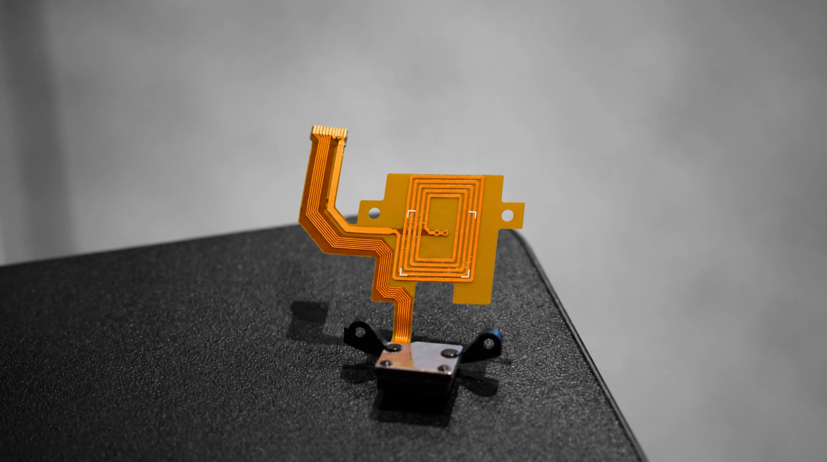
Flex PCBs are one step in this evolution. By combining the functionality of a PCB with the adaptability of a cable, they allow circuits to follow the shape of a product and create more freedom in its design.
But greater design freedom brings new engineering decisions. Reliability, cost, manufacturing complexity and serviceability can change as electronics become part of the product itself. The opportunity is to use these technologies where they unlock real value, while ensuring the resulting product remains practical to build, use and maintain.
What is a Flex PCB?
Traditional PCBs are built on a rigid, flat substrate – a simple, robust approach that works well for most electronic products. A flex PCB uses a thin flexible substrate, allowing conductive layers to form a circuit that can bend and conform to the structure around it. It can replace wiring between different parts of an assembly, reducing the need for separate cables and connectors. The benefits are clear: less space, lower weight and potentially simpler assembly. But there are trade-offs.
Replacing a rigid board with a flexible one is not a simple drop-in replacement. Bend radius, component placement and mechanical stress all become part of the design challenge. A circuit that performs perfectly when stationary may behave differently when repeatedly flexed during normal use. Engineers need to understand how the circuit will behave throughout the product’s life cycle. Where will the mechanical stress concentrate? How will the board be assembled, supported and handled? Can components and copper tracks withstand the expected movement? There are also manufacturing and commercial considerations. Flex PCBs may reduce the number of connectors and cables, but their fabrication and assembly can introduce additional complexity. Manufacturing tolerances, component mounting and assembly processes all influence both cost and reliability.
The real benefit needs to be assessed across the entire manufacturing process, from yield and assembly to testing and long-term serviceability. In a design that bends repeatedly, even the position of copper within the flex stack-up matters. Placing conductors nearer the neutral bend axis can reduce strain, which is why the circuit layout and mechanical design need to be developed together. Sometimes, the best solution is a hybrid design, combining rigid and flex. This approach can deliver many of the benefits of flex PCBs without adding unnecessary complexity across the entire design.
That is what makes flex PCBs interesting: they do more than change the shape of the circuit board. They can enable product forms that would otherwise be difficult to achieve, while bringing mechanical design into the way we think about electronics.
Beyond the Flex PCB
Flex PCBs solve one problem. But what happens when the surface starts to move? What if the circuit needs to stretch? Or twist? This is where stretchable electronics enter the picture.
Using conductive inks, stretchable conductors and geometries such as serpentine traces, these circuits can move with the surface they are attached to, rather than simply bending around it. Imagine a wearable device positioned over a joint – as the joint moves, the electronics need to stretch and flex with it, again and again throughout everyday use. This creates an opportunity to design the electronics, surface and mechanical structure as a single system, enabling sensing and interaction in places where a conventional board may not fit.
However, printed electronics are not a straightforward replacement for conventional copper circuits. Conductivity, material adhesion, and manufacturing repeatability all influence performance. In stretchable designs, repeated deformation can place stress on interconnections and gradually degrade electrical continuity. Material selection and circuit geometry matter. Engineers need to balance conductivity, durability and consistent performance, while considering whether a design that works in an initial prototype continues to perform after thousands of movement cycles.
Another approach takes integration a step further: in-mould electronics (IME). IME integrates conductive paths, sensors and other electronics directly into three-dimensional moulded parts. Automotive interiors are one example. Capacitive touch controls and ambient lighting can be integrated into interior components, reducing the need for separate switches and electronic assemblies. The result can be a clean, seamless surface that combines functionality with product design.
But integrating electronics into a moulded part changes how the part is manufactured. Forming and moulding conditions, inspection access and production yield all need careful consideration. If a defect is detected after the electronics have been integrated into a finished component, reworking or scrapping can be costly. An early design question is how the electronics will be tested before they are moulded in. Detecting a fault at that stage can mean rejecting a printed circuit rather than an entire finished component. The same broader trend towards flexible product design is seen in consumer electronics. Flexible and foldable displays, for example, use flexible materials and a multilayer structure designed to withstand repeated changes in shape.
These technologies aren’t interchangeable, and not all products need the most advanced approach. In some cases, a conventional PCB remains the right choice. In others, a combination of rigid PCBs with flexible interconnections or a moulded interface offers a genuine advantage. The opportunity is to create a better fit between electronic functionality and the application. The challenge is to achieve that without introducing disproportionate cost, manufacturing or serviceability penalties.
Electronics You Can Wear
The human body may be one of the most interesting places to apply these technologies. Unlike most products, the surface is consistently moving, creating unique challenges for conventional electronics. Most wearable devices still rely on compact electronics attached to a watch, patch or garment. But stretchable electronics offer another possibility – distributing the sensing elements and conductive pathways across a surface that moves with the body. Imagine clothing that monitors movement, posture or environmental conditions without requiring a separate device. Or a thin patch that sits against the skin and collects data as the body moves.
A patch-style biosensor is one example. Its sensing element could be printed directly onto a flexible substrate, creating a thin, lightweight sensing platform. Depending on the sensing technology, this could support continuous, non-invasive monitoring without the bulk of a conventional device. But getting a sensor to work in a prototype stage is only the first step. Can it deliver consistent measurements while the wearer moves and perspires? Will it remaiprototype stagen comfortable and attached during extended use? How will motion artefacts, skin compatibility and environmental exposure affect its performance?
For medical applications, all these questions need to be considered alongside electrical safety, verification and validation, the intended product life and the conditions in which the device will be used. The sensing element, attachment method, signal processing, and manufacturing process must all be considered in product design and work together as a system.
There is also the challenge of scaling production. A wearable sensor that performs well in a small prototype run may not deliver the same consistent result across large production volumes. Variations in printed features, material properties and assembly processes can affect manufacturing yield and product consistency. In other words, demonstrating that a technology works is only the beginning. Making it reliable, repeatable and economically viable is what turns a promising concept into a product.
The goal is not simply to make a smaller device. It is to make electronics that fit naturally into the way we live, move and interact with the world.
The Opportunity and the Engineering Trade-offs
Flexible, printed and embedded electronics offer more than alternatives to rigid circuit boards. They can put sensing and control into moving surfaces, clothing and moulded parts, enabling capabilities and product experiences that conventional approaches struggle to deliver. The opportunity must be weighed against the demands of the application. Electrical and mechanical performance, manufacturing yield, cost and serviceability can all determine whether an innovative concept becomes a viable product.
At Ingenuity, we bring electronic, mechanical, industrial design and manufacturing expertise together early to explore these possibilities and resolve the trade-offs. The aim is to turn new capabilities into products that work reliably and deliver meaningful value.