Avoiding Pitfalls: Expert Tips for Reliable, Manufacturable PCB Designs

.jpg)
In the world of electronics, a well-designed printed circuit board (PCB) can make or break a product. While it might seem as simple as connecting components with traces, the reality is far more intricate. Successful PCB design requires a deep understanding of electromagnetic compatibility (EMC), noise reduction, power distribution, and manufacturability. By mastering these elements, designers can avoid common pitfalls and create reliable, high-performance boards.
1. Optimizing for EMC
To minimize electromagnetic emissions, it's crucial to reduce the loop area of conductors, especially those connected to high-frequency components with rapid edge rates. Optimizing ground planes for continuity and selecting an appropriate stack-up are essential for minimizing EMC. Additionally, maintaining trace impedance, trace length matching and considering appropriate termination networks are important for signal integrity and further mitigating EMI.
2. Reducing Noise Interference
Proper component placement is vital. Keep sensitive analog inputs away from noisy outputs and power supplies. Employing isolated ground planes and strategic routing can prevent unwanted coupling and crosstalk. Utilizing decoupling capacitors close to IC power pins, and strategic use of ferrite beads and chokes can also suppress noise.
3. Power Distribution Considerations
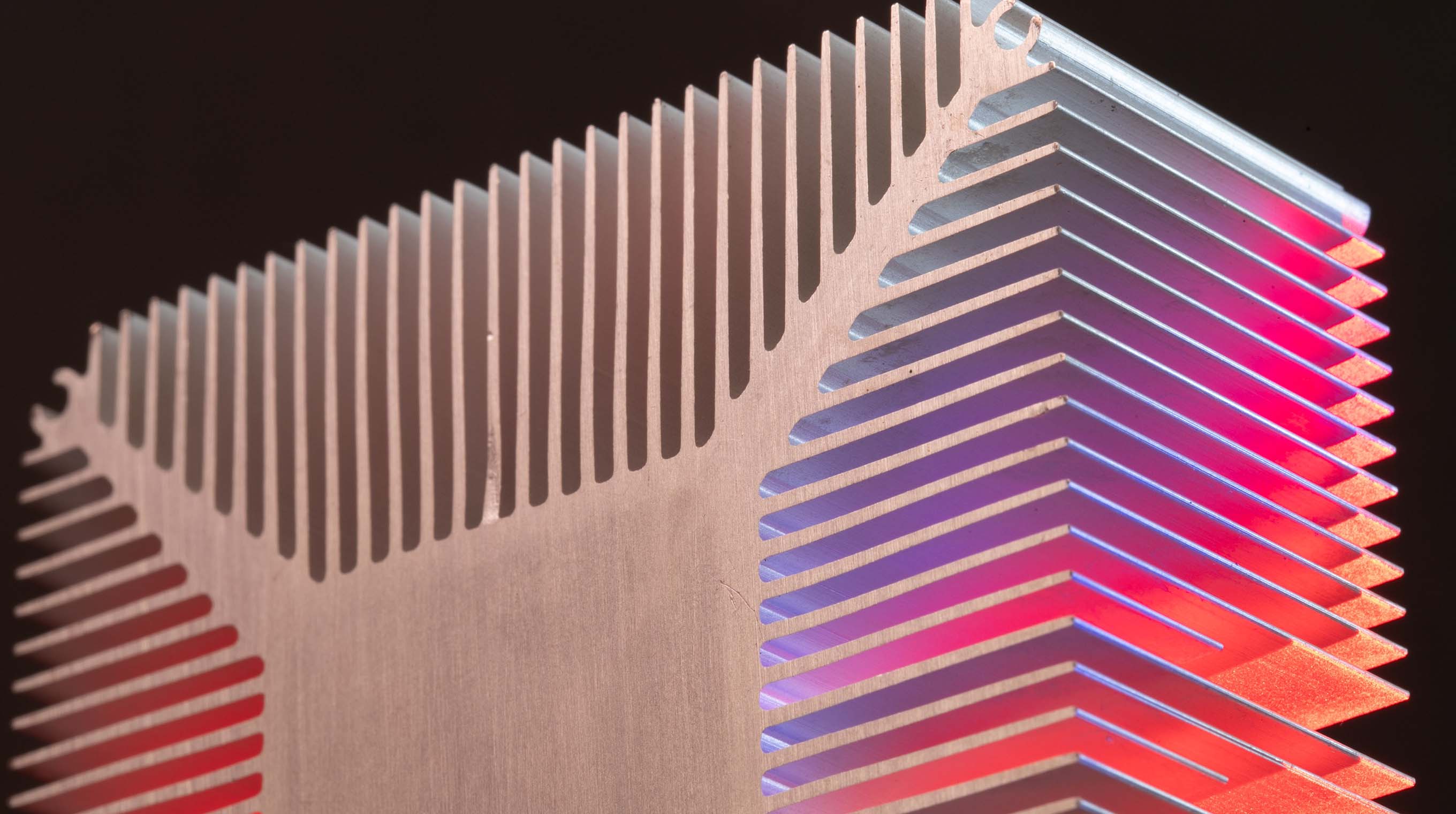
High-current traces should be wider to handle the load, increase ground coupling and reducing emissions. Keeping these traces short and direct helps avoid unnecessary voltage drops and ensures efficient power distribution. Implementing a well-designed power distribution network with proper filtering and decoupling networks can reduce power noise and provide stable power, minimizing its impact on signal quality. Additionally, PCB layout needs to consider thermal aspects including appropriate heat sinking and thermal relief.
4. Design for Manufacture
Manufacturability starts with adhering to well-defined PCB design rules—including clearances, annular ring dimensions, solder mask expansion, and ground pour pullback—tailored to your manufacturer’s capabilities. In high-density designs, special attention must be paid to the use of blind and buried vias. Beyond that, decisions around layer stack-up, panelization, and component placement all play a critical role in determining production cost and complexity. Testability can be enhanced by incorporating features such as test points and edge connectors. By addressing these considerations early in the design process, you can ensure a PCB that is both reliable and economical to produce.
In conclusion, PCB design is not merely about connecting components; it involves creating a reliable, interference-free, and cost-effective board. By considering these factors, you can avoid common pitfalls and achieve a successful design.