GaN Thermal Design: Beyond the Heatsink

GaN has redefined what’s possible in power electronics, especially for high-voltage systems.
Some of its qualities include higher switching speeds, smaller magnetics, and increased power density. Not to mention more compact systems.
But those gains come with a trade-off: significantly tighter thermal margins. Meaning, less design buffer for heat management.
When thermal impacts are underestimated in a GaN-based system, the consequences can be serious. Elevated temperatures reduce efficiency, shorten device lifetime, and in severe cases, cause catastrophic failure. In compact power stages, there is very little room for error.
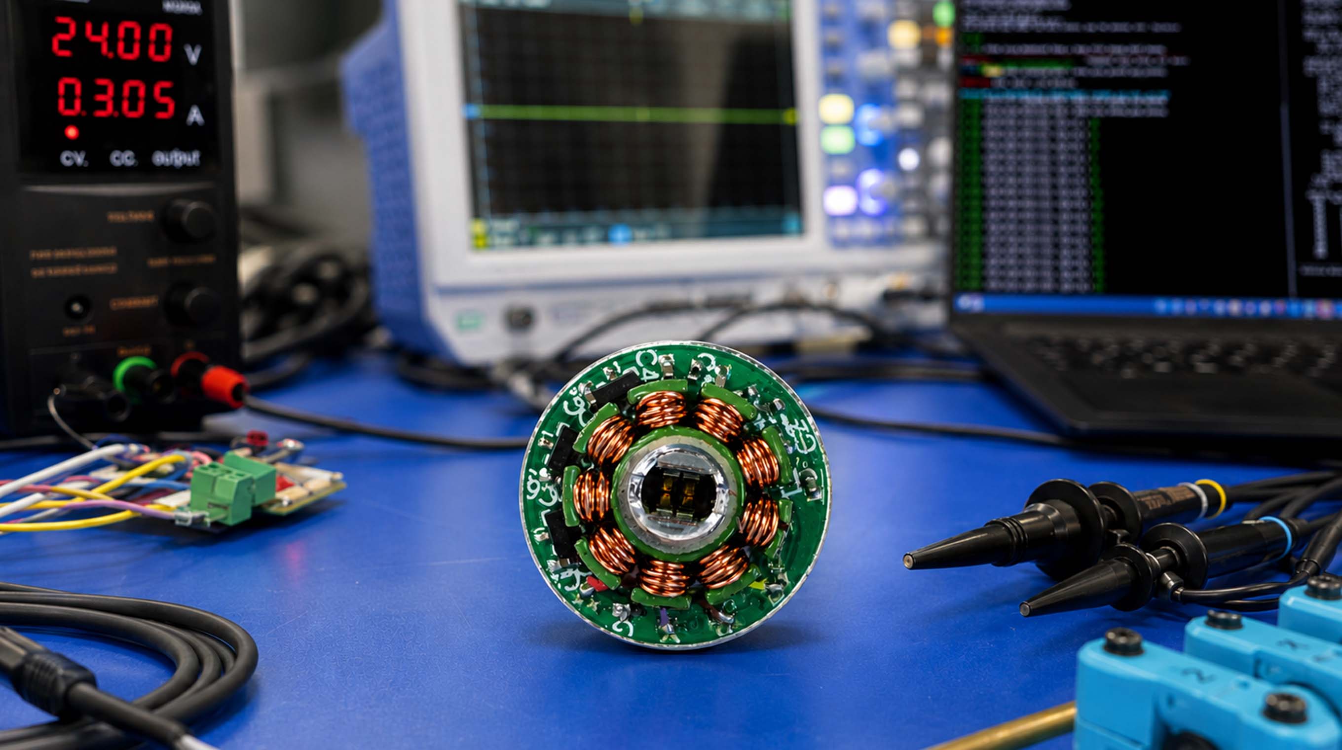
At Ingenuity Design Group, one of our early hands-on lessons with GaN came from developing a top-side heatsink solution for a compact, high-density power stage. What we learned reinforced a critical truth: Thermal performance is a system outcome, rather than a component choice.
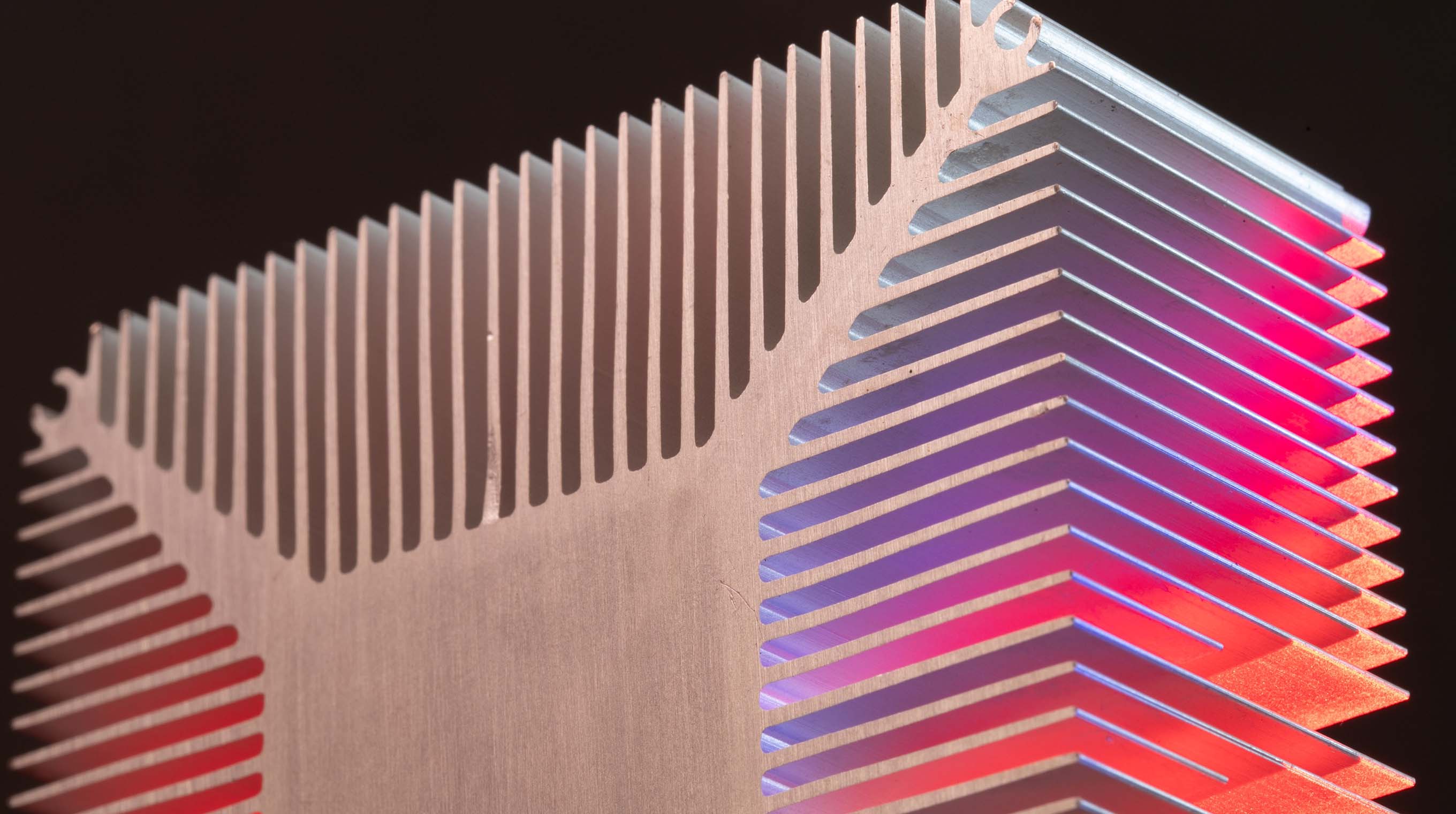
The Full Heat Path Determines Success
A common mistake in high-density power design is to focus on the heatsink as the primary solution. In reality, heat leaves a GaN device through multiple paths. Typically, heat flows both into the PCB and into the top-side cooling path.
A top-side heatsink can be highly effective. It performs best when the PCB is also engineered to spread and conduct heat efficiently. In compact GaN power stages, very high currents may need to be routed through limited PCB area, making copper loss, current density, and board-level heat spreading major design constraints.
Solutions include more copper layers, heavier copper, thermal vias, and wider planes, which can all help distribute heat. In our findings, the heatsink can remove heat from the PCB through thermal interface material, creating an additional PCB-to-heatsink path and reducing the burden on copper alone.
If either the device-to-heatsink path or the PCB-to-heatsink path is weak, overall thermal resistance increases and margins disappear quickly.
At Ingenuity Design Group, we approach GaN thermal architecture as a fully integrated system from the outset. The most robust designs treat all available heat paths as a single, coordinated strategy from day one.
The Interface Layer Can Make or Break Performance
One of the most significant lessons from our development work at Ingenuity Design Group was how much the thermal interface material (TIM) influences real-world results.
With compact GaN packages, the contact area is small. That makes bond-line thickness and interface quality disproportionately important. Even with an optimized heatsink, thermal performance drops rapidly if TIM thickness is uncontrolled, contact pressure is uneven, or compression varies between builds.
TIM selection also has an electrical dimension. In high-voltage systems, such as designs with nodes above 60 V, the interface material may need to provide electrical isolation between the power stage and the heatsink. Dielectric strength, breakdown voltage, material thickness, compliance, and long-term reliability must be considered alongside thermal conductivity.
Thermal resistance introduced at the interface is often invisible in early modelling but highly visible in hardware testing. This is where experience becomes critical to understand what will remain safe, repeatable, and consistent in production.
Spacers Are Precision Thermal and Mechanical Hardware
In our top-side heatsink architecture, spacers became a defining element of the thermal solution.
They controlled the physical gap between device and heatsink, TIM bond-line thickness, assembly compression force, and the mechanical load applied to the top side of the GaN devices.
Top-side cooling is also a structural challenge. Compact GaN packages can be sensitive to excessive mechanical pressure. Too little compression can create poor thermal contact; too much compression can overstress the package, damage the device, or compromise long-term reliability.
Without proper stack-up control, tolerances compound. Variations build from PCB thickness, device height, and mounting hardware. The result is inconsistent thermal performance from unit to unit, among other problems.
Spacers, in this context, are precision thermal and mechanical control features - and at Ingenuity Design Group, they are treated accordingly.
The PCB Still Carries a Major Thermal Burden
Even in a top-cooled architecture, the PCB remains a primary thermal pathway.
As most hardware engineers know all too well, board-level decisions directly influence heat spreading capability, including copper weight and plane area. Key decisions to be made include, thermal via density and placement, local component density and available board real estate around the device.
In high-current GaN designs, the PCB is carrying more than signals and interconnects. It may also carry substantial power current through very compact geometry, creating additional thermal challenges from copper conduction losses and limited area for heat spreading.
In some compact architectures, coupling the PCB thermally to the heatsink through an appropriate TIM provides another heat extraction path and improves overall system performance.
That approach must be engineered carefully. The material has to meet the thermal, mechanical, and electrical requirements of the system, including any required isolation between high-voltage circuitry and accessible or chassis-connected metalwork.
In compact designs, these details often determine whether a product merely survives lab testing or performs reliably over years of operation.
This is why Ingenuity Design Group integrates electronics, mechanical, and thermal considerations early, from the beginning of the design process.
Expertise Is Essential in High-Density GaN Design
Top-side heatsinking can be an excellent solution for GaN-based systems, particularly where space is constrained and performance targets are aggressive.
The interaction between PCB design, interface materials, stack tolerances, mounting strategy, electrical isolation, mechanical loading, and system airflow forms a tightly coupled thermal network.
The lessons we continue to apply at Ingenuity Design Group are clear:
- Design the full heat path, rather than just the heatsink.
- Treat TIM, spacer control, and mechanical stack-up as critical thermal and reliability elements.
- Consider electrical isolation requirements when selecting thermal interface materials.
- Use the PCB as an active heat-spreading structure.
- Engineer for repeatable assembly from the beginning.
GaN technology delivers extraordinary performance potential. Realizing that potential safely and reliably requires integrated, multi-disciplinary engineering expertise.
At Ingenuity Design Group, we partner with clients to ensure advanced power electronics systems achieve peak performance.

.jpg)